
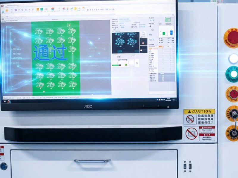
Reliable solder joints begin before reflow. Our Solder Paste Inspection (SPI) solution helps electronics teams verify paste deposits early, reduce preventable defects, and keep PCB assembly moving with clearer process data. Built for manufacturers working across Consumer Electronics, Industrial Electronics, Automotive Electronics, Communications & Networking, Electronics Manufacturing Services (EMS), and Medical Devices, it turns solder paste testing into a controlled, repeatable step instead of a last-minute quality check.
What Does This Solder Paste Inspection (SPI) Solution Include?
It includes a practical inspection workflow for checking solder paste presence, volume, area, height, position, bridging risk, and other paste-related conditions before components are placed. The system is designed to support SPI solder paste inspection on modern PCB assemblies where pad size, pitch, and production speed leave little room for guesswork. Instead of relying only on visual review or post-reflow inspection, teams can catch paste issues while boards are still recoverable.
Designed to Catch Paste Defects Before They Become Assembly Failures
Solder paste problems often appear small at first: a deposit slightly off pad, insufficient paste on a fine-pitch device, excess paste between terminals, or inconsistent release from a stencil aperture. After reflow, those issues can become opens, shorts, tombstoning, voiding concerns, intermittent connections, or expensive rework. A focused SPI process helps operators see these risks at the point where corrective action is still practical.
This page is for teams evaluating inspection equipment and PCB inspection tools that can support tighter process control. Whether you run high-mix EMS work or dedicated production for regulated electronics, SPI adds measurable discipline to the printing stage. It gives process engineers and quality teams the information they need to adjust stencil cleaning, squeegee pressure, paste condition, board support, printer alignment, and other variables that influence print quality.
Core Inspection Techniques Supported by the Workflow
A strong SPI program uses more than a pass/fail image. It combines measurement, defect detection, process monitoring, and traceable review so that production teams can understand both the board and the process behind it.
- Presence and absence checks: Confirms that solder paste is deposited where expected and flags missing deposits before placement.
- Volume measurement: Helps identify insufficient or excessive paste that may affect joint formation after reflow.
- Height and area analysis: Shows whether paste deposits are consistent across pads, components, and board regions.
- Offset detection: Highlights paste that has shifted from the target pad location and may increase bridge or open-joint risk.
- Bridge and smear detection: Looks for paste connecting adjacent pads, especially on fine-pitch devices.
- Trend review: Supports process improvement by showing whether defects are isolated events or part of a wider print issue.
- Operator review tools: Gives production staff a clearer basis for board disposition than manual visual inspection alone.
These techniques help turn solder paste testing into actionable feedback. Instead of discovering the same defect downstream, teams can respond at the print stage and prevent repeated failures across a batch.
Practical Benefits for PCB Production Teams
The main value of SPI is not only defect detection. It is faster decision-making at the most influential point in the SMT process. When a paste print is wrong, every later step adds cost and complexity. Inspection before component placement helps protect materials, labor, schedule, and customer confidence.
For production managers, SPI supports more stable throughput by reducing avoidable interruptions later in the line. For process engineers, it provides data that can guide printer setup and maintenance. For quality teams, it creates a stronger record of how PCB soldering standards are supported through controlled inspection activity rather than informal judgment.
Key benefits include:
- Earlier defect containment before components and reflow add cost.
- More consistent print process control across operators, shifts, and product builds.
- Better visibility into recurring print issues such as clogged apertures, stencil wear, poor board support, or paste handling problems.
- Reduced dependence on subjective visual checks for fine-pitch and dense PCB layouts.
- Stronger production documentation for customers who expect disciplined electronics manufacturing processes.
- Improved feedback between printing, inspection, and engineering when defects need root-cause review.
A Fit for Demanding Electronics Markets
Different industries have different risk profiles, but they all depend on reliable solder formation. In Consumer Electronics, dense layouts and fast production cycles demand quick, repeatable inspection. In Automotive Electronics, consistent process control matters because products may be exposed to vibration, temperature variation, and long service expectations. In Medical Devices, manufacturers often need clear documentation and careful control of process variation.
Communications & Networking products may include complex boards with many interconnects, shielding considerations, and high-density assemblies. Industrial Electronics can involve varied board types, lower-volume builds, and long product lifecycles, making repeatability especially important when a job returns months later. Electronics Manufacturing Services (EMS) providers benefit from flexible PCB inspection tools that can adapt across customer programs without turning every new build into a custom inspection challenge.
Built to Support Operators, Engineers, and Quality Teams
Inspection equipment works best when it fits the real production environment. Operators need clear calls, usable images, and simple review steps. Engineers need measurement data that can point to the likely source of variation. Quality teams need inspection records that support accountability without slowing production unnecessarily.
This SPI approach is built around those shared needs. It supports routine board inspection while also helping teams investigate why a printer is drifting, why a specific package type is generating defects, or why paste deposits vary across the panel. The goal is not to create more data for its own sake; it is to make the print process easier to understand and control.
Feature Overview
A well-implemented Solder Paste Inspection (SPI) system should make complex inspection easier to apply on the line. The following capabilities help teams move from reactive checks to proactive process control.
| Feature | What It Helps You Do | Practical Production Value |
|---|---|---|
| 2D and 3D inspection workflow | Review paste shape, coverage, and deposit condition | Improves confidence beyond basic visual checks |
| Measurement-based defect calls | Evaluate volume, height, area, and offset | Supports more consistent pass/fail decisions |
| Program setup tools | Create inspection routines for different PCB assemblies | Helps high-mix lines change over more smoothly |
| Defect classification | Identify missing paste, excess paste, bridges, and misalignment | Speeds review and corrective action |
| Process trend visibility | Watch patterns across boards, panels, or shifts | Helps engineers address root causes |
| Review and reporting functions | Document inspection outcomes | Supports quality expectations and customer communication |
Because every production line is different, final configuration, integration, and reporting needs should be matched to the boards you build, the throughput you require, and the internal standards you follow.
How SPI Improves a Typical Print-Stage Decision
Consider a board with fine-pitch components and several large thermal pads. Without SPI, a paste issue may not be obvious until after reflow, when repair is slower and the cause may be harder to isolate. With inspection before placement, the team can see whether the issue is a missing deposit, too much paste, an offset print, or inconsistent release from the stencil.
That changes the decision. The operator can stop a questionable board before more value is added. The engineer can review whether the defect appears in one location or across the panel. The quality team can document the result and confirm whether the process is still aligned with internal PCB soldering standards.
Implementation Path for Your Line
Adding SPI should be deliberate, not disruptive. The best results come from connecting the inspection plan to the actual product mix and the defects that matter most to your operation.
- Review your PCB assemblies and risk points. Identify fine-pitch parts, small passives, high-value boards, and components with known solder sensitivity.
- Define inspection priorities. Decide which paste conditions require immediate stop, operator review, or engineering escalation.
- Set up inspection programs. Build routines around pad geometry, component type, and expected paste behavior.
- Train operators on review decisions. Make sure the team understands what to accept, what to reject, and when to ask for support.
- Use data for process improvement. Review trends to refine stencil cleaning, printer setup, paste handling, and maintenance.
This structure keeps SPI tied to production value. The system becomes more than a checkpoint; it becomes part of continuous improvement.
Pricing and Configuration
Pricing depends on configuration, production requirements, software needs, integration scope, and support expectations. Because PCB assemblies vary widely, a quote-based approach is the most accurate way to match the solution to your line. The right package may differ for a high-volume Consumer Electronics line, a flexible EMS environment, or a Medical Devices manufacturer with added documentation needs.
To prepare for a quote, gather details such as board dimensions, component density, current printer setup, expected throughput, preferred reporting needs, and any applicable customer or internal quality requirements. Sharing example boards or common defect concerns can also help define the most useful inspection setup.
Move from Paste Inspection to Paste Control
Solder paste inspection is most valuable when it helps your team act sooner, learn faster, and build with greater consistency. The right SPI system gives operators clear calls, engineers useful process insight, and quality teams stronger documentation. If you are evaluating inspection equipment or upgrading PCB inspection tools, this solution provides a practical path toward better print-stage control.
Request a consultation or quote to discuss your PCB assemblies, production goals, and solder paste testing requirements. We will help you identify a configuration that fits your line without adding unnecessary complexity.
FAQ
What is Solder Paste Inspection (SPI)?
Solder Paste Inspection (SPI) is an inline quality control process that measures solder paste volume, height, area, and alignment after printing but before component placement. It catches print defects early, when corrective action is still practical.
Why is SPI important in SMT assembly?
Research shows that 50–70% of solder defects originate from the printing process. SPI helps catch issues like insufficient paste, excess paste, bridging, and misalignment before reflow, reducing rework and improving first-pass yield.
What is the difference between SPI and AOI?
SPI inspects solder paste immediately after printing, before components are placed. AOI inspects the board after reflow, checking component presence, placement, and solder joints. SPI catches print defects early; AOI catches assembly defects later.
Which industries use Solder Paste Inspection?
SPI is widely used in Consumer Electronics, Automotive Electronics, Medical Devices, Industrial Electronics, Communications & Networking, Aerospace, and EMS providers — anywhere solder joint reliability matters.
What defects can SPI detect?
SPI detects missing paste, insufficient or excessive paste, offset deposits, bridging between pads, smearing, and inconsistent release from stencil apertures. These are the root causes of opens, shorts, tombstoning, and voiding after reflow.
Need reliable Solder Paste Inspection for your PCBA production?
Greenspcba Technology integrates SPI, AOI, X-ray, and functional testing into our SMT PCBA and medical electronics manufacturing processes. From prototype to production, we help you catch defects before they reach your customers. Contact us with your BOM and Gerber files for a 24-hour quote.
Recent Comments