
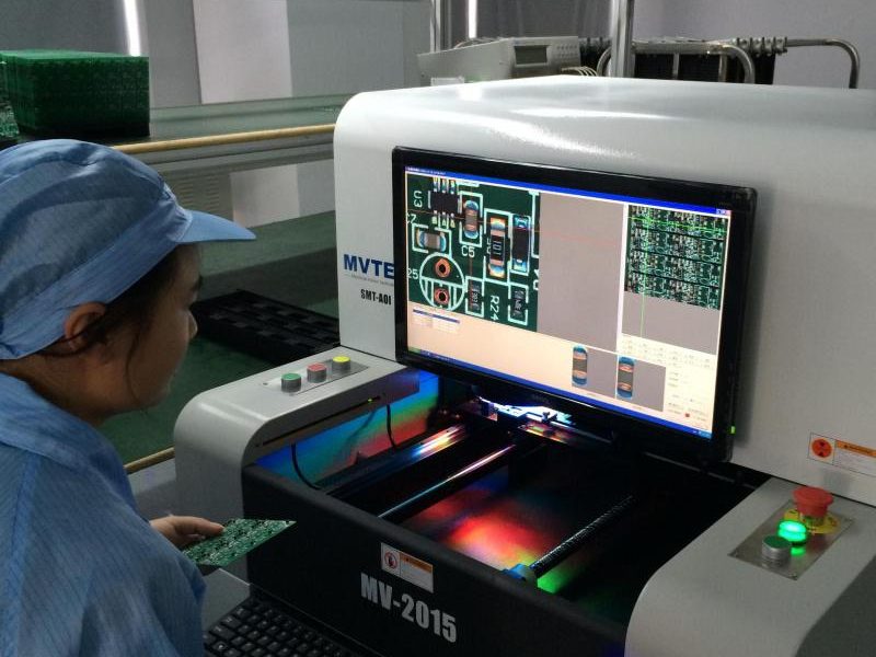
Modern optical inspection helps electronics manufacturers find defects earlier, verify process stability, and protect product quality before boards move further down the line. For Electronics Manufacturing Services (EMS) providers, OEMs, and production teams, the right mix of aoi inspection equipment, machine vision, image analysis, and complementary test methods can reduce manual review burden while giving quality teams clearer evidence for action.
If your inspection process still depends heavily on slow visual inspection, inconsistent operator judgment, or late-stage troubleshooting, automated inspection can create a stronger quality control foundation. This page outlines what today’s optical inspection technologies do, where they fit in PCB manufacturing, and how to think about choosing the right approach for your operation.
What can modern optical inspection do for your production line?
Modern optical inspection can examine PCB assemblies, solder joints, component presence, polarity, markings, placement, and surface-level workmanship using cameras, lighting, software, and repeatable inspection rules. In practical terms, aoi automated optical inspection helps teams detect issues closer to the point of origin, instead of waiting until final test, customer returns, or downstream rework reveals a problem.
For an EMS environment, that matters because one assembly line may run multiple products, each with different board layouts, component packages, and acceptance criteria. Automated optical inspection pcb workflows give quality teams a repeatable way to check critical features while still allowing trained staff to review exceptions and make process decisions.
Inspection built for modern PCB complexity
As PCB assemblies become denser, manual inspection becomes harder to rely on as the primary safeguard. Smaller components, fine-pitch packages, hidden terminations, varied board finishes, and high product mix can make defects difficult to spot consistently with the naked eye. AOI PCB systems address this challenge by combining controlled lighting, high-resolution imaging, measurement tools, and defect classification software.
This does not mean human expertise disappears. Instead, automated inspection gives experienced operators and engineers better information. A technician no longer has to scan every board feature from scratch; they can focus on flagged conditions, trend patterns, and process corrections that require judgment.
In a well-planned quality control process, optical inspection supports decisions such as whether a printer needs adjustment, whether a placement issue is developing, or whether soldering parameters should be reviewed. The value is not only defect detection. It is faster feedback.
Core capabilities that improve quality control
The strongest inspection programs combine hardware, software, process knowledge, and disciplined review. When aoi inspection pcb systems are configured around the actual risks of a product, they can help teams standardize inspection and respond before small process shifts become expensive failures.
Key capabilities include:
- Automated defect detection: AOI can check for missing components, wrong parts, skew, tombstoning, bridges, insufficient solder, excess solder, lifted leads, polarity issues, and visible contamination concerns when the inspection setup supports those checks.
- Image analysis for consistent review: Software compares captured images against programmed expectations, inspection libraries, or reference data, helping reduce variation between shifts and operators.
- Machine vision measurements: Precision measurement tools can evaluate locati0n, shape, height-related visual cues, spacing, and other visible characteristics that are hard to judge consistently by eye.
- Process traceability: Inspection images and defect records can support root cause analysis, supplier discussions, internal quality reviews, and continuous improvement work.
- Flexible program adjustment: For EMS teams handling changing product demand, AOI programs can be refined as assemblies, tolerances, and known risk points change.
These capabilities are most useful when inspection rules are meaningful. Overly loose settings can let defects pass. Overly tight settings can create false calls and slow production. The goal is a balanced inspection strategy that supports reliable decisions.
From manual visual inspection to automated optical inspection
Traditional visual inspection still has a role, especially for unusual conditions, cosmetic review, and engineering judgment. However, relying on manual inspection alone can create bottlenecks and inconsistent outcomes. Fatigue, lighting differences, board complexity, and varying inspector experience all affect results.
AOI automated optical inspection brings repeatability to the inspection process. The system captures images under controlled conditions and applies defined criteria to each board. That creates a more stable baseline for quality control and allows human reviewers to concentrate on verification, disposition, and process improvement.
A common before-and-after scenario is easy to recognize. Before AOI, a team may discover solder bridge trends during functional test, after multiple boards have already passed through later production steps. With an automated optical inspection pcb process placed closer to soldering or placement, the same trend can be flagged earlier, giving engineers a chance to correct the process before additional assemblies require rework.
Where AOI fits in a complete test strategy
Optical inspection is powerful, but it is not the only inspection or test method a reliable production line needs. AOI is best used as part of a layered strategy that may also include automated x ray inspection, in circuit test, functional test, boundary scan, and targeted manual review.
Each method answers a different question:
- AOI PCB inspection helps identify visible defects on the board surface, including component and solder-related conditions that cameras can evaluate.
- Automated x ray inspection is useful when joints or features are hidden, such as under certain area-array packages or shielded locations.
- In circuit test checks electrical characteristics and can reveal problems that are not visible through optical inspection alone.
- Functional test verifies whether the completed assembly performs as intended in its application or simulated operating conditions.
- Human review provides contextual judgment for ambiguous findings, cosmetic standards, unusual assemblies, and engineering evaluations.
A stronger quality plan does not treat these methods as competitors. It uses each method where it adds the most value. AOI can reduce the number of defects reaching electrical test, while electrical and functional methods can catch issues optical systems cannot see.
Technology advances that make inspection smarter
Advancements in optical inspection are not limited to sharper cameras. The real improvement comes from the way imaging, lighting, algorithms, data, and operator workflows work together. Better image capture can reveal more detail, but better software and process integration help teams act on that detail.
Modern systems may support multi-angle imaging, advanced illumination, 2D and 3D inspection approaches, improved component libraries, and more efficient false-call management. These features can help with complex solder geometries, reflective surfaces, small packages, and dense board areas where simple image comparison may not be enough.
Image analysis also supports continuous improvement. When defect data is reviewed over time, teams can identify recurring issues by product, process step, supplier lot, component type, or shift. That turns inspection from a pass-fail checkpoint into a source of manufacturing intelligence.
For EMS providers, this is especially valuable. A high-mix production environment needs flexible systems that can support different assemblies without requiring quality teams to start from zero every time. The better the inspection workflow, the easier it is to balance speed, accuracy, and documentation.
Practical benefits for EMS and OEM teams
A strong automated inspection process supports both production efficiency and customer confidence. It helps EMS providers demonstrate that inspection is not an afterthought; it is built into the manufacturing flow.
For production leaders, benefits often include:
- Earlier defect discovery: Problems can be identified near the process step that created them, reducing downstream disruption.
- Reduced dependence on manual screening: Operators can spend more time reviewing exceptions and less time performing repetitive checks.
- More consistent quality control: Defined inspection criteria help reduce variation between people, shifts, and product runs.
- Better rework prioritization: Clear defect images and classifications help teams decide what needs immediate attention.
- Improved customer communication: Inspection records can support transparent discussions about quality expectations, corrective actions, and process controls.
- Stronger process learning: Trend data helps teams move from reacting to individual defects toward preventing repeat issues.
These benefits depend on thoughtful implementation. The best equipment cannot compensate for unclear acceptance criteria, poor program maintenance, or inspection data that nobody reviews.
How to choose the right inspection approach
Selecting aoi inspection equipment starts with the product, not the brochure. A simple board with large components may not require the same inspection depth as a dense assembly with fine-pitch devices and hidden solder joints. The right solution depends on board complexity, defect risks, throughput needs, documentation requirements, and how inspection results will be used.
Before investing in or upgrading AOI, consider:
- Assembly risk profile: Identify which defects are most likely, most costly, or most difficult to detect later.
- Inspection locati0n: Decide whether AOI should be placed after paste printing, component placement, reflow, selective solder, wave solder, or final assembly.
- Data requirements: Determine what images, measurements, reports, and traceability records your team or customers need.
- Review workflow: Plan who will verify calls, disposition defects, update programs, and monitor false-call rates.
- Complementary testing: Decide where automated x ray inspection, in circuit test, and functional testing are needed to cover what optical inspection cannot.
This planning step prevents a common problem: buying inspection capability without building an inspection process. The technology works best when it is tied to clear standards, trained users, and a defined response when defects are found.
Turn inspection into a competitive advantage
Optical inspection is no longer just a final check for visible defects. Used well, it becomes a practical quality control system that improves feedback, supports documentation, and helps manufacturing teams keep pace with modern PCB complexity. For EMS providers and OEM production teams, that can mean fewer surprises, clearer decisions, and a more disciplined path from build to shipment.
If you are evaluating aoi automated optical inspection, improving an existing AOI PCB process, or building a broader inspection strategy around automated inspection, now is the right time to review where defects are found and where they should be found. Start by mapping your current inspection points, the defects that escape them, and the test methods needed to close the gaps.
Ready to strengthen your PCB inspection workflow? Contact Greenspcba Technology request a consultation or inspection process review to identify where optical inspection, machine vision, automated x ray inspection, and in circuit test can work together to support more reliable production.
Recent Comments