
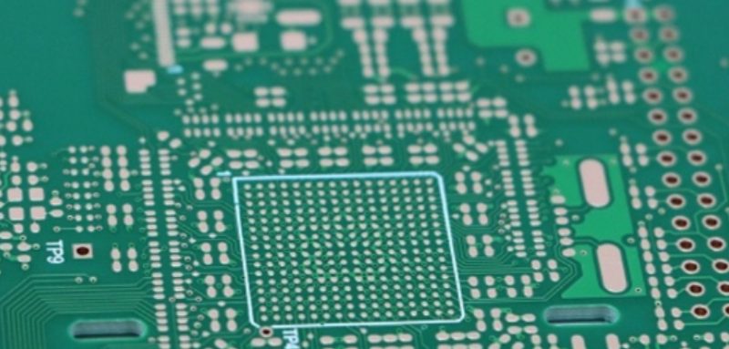
Professional electronics manufacturer are putting renewed emphasis on disciplined PCB design as products become smaller, faster, and more connected. The latest focus is not only on choosing better pcb design software, but also on building a design process that reduces rework before fabrication. For engineers, students, and product teams, the message is clear: effective design for PCB work now depends on planning, verification, manufacturability, and practical learning—not layout speed alone.
What should engineers focus on first?
Engineers should begin with requirements, constraints, and component placement before routing a single trace. A clean schematic, realistic board outline, defined layer stack, power needs, signal priorities, and manufacturing limits create the foundation for every later decision. When teams skip this early structure, even strong pcb design tools cannot fully compensate for unclear intent, crowded routing, poor thermal planning, or avoidable fabrication issues.
That early discipline is especially important for teams moving from simple prototypes to compact, production-ready boards. A board that works once on the bench may still be difficult to manufacture, test, repair, or scale. Effective PCB design now means thinking about the full path from schematic capture to assembly, inspection, enclosure fit, and field reliability.
Tool choice is becoming a workflow decision
The market for pcb design software gives engineers more options than ever, but the best choice depends on project complexity and team workflow. Entry-level users may need intuitive schematic capture, clear design-rule setup, and strong tutorials. Professional teams often look for collaboration features, version control integration, advanced routing, impedance tools, library management, and manufacturing output checks.
The practical shift is that pcb design tools are no longer just drawing environments. They increasingly sit at the center of engineering communication. A well-managed project file can connect electrical design, mechanical fit, procurement, fabrication, testing, and revision history. That reduces confusion when a board changes after prototype feedback.
Useful software features to evaluate include:
- Design-rule checking: Helps catch spacing, clearance, width, and via issues before manufacturing files are released.
- Library control: Keeps footprints, symbols, and part data consistent across projects.
- 3D board preview: Supports enclosure checks, connector alignment, and mechanical coordination.
- Manufacturing file export: Produces Gerber, drill, pick-and-place, and bill-of-materials data in a controlled way.
- Simulation or analysis support: Helps review signal, power, or thermal behavior when the project requires it.
- Collaboration tools: Allows multiple engineers, reviewers, or manufacturing partners to work from the same source of truth.
No single tool fixes weak design habits. However, the right tool can make good habits easier to repeat.
Better placement still drives better routing
Experienced PCB designers continue to treat component placement as one of the most important stages of the process. Good placement shortens critical routes, reduces crossing signals, improves current paths, and makes the board easier to inspect. Poor placement creates routing pressure that often leads to unnecessary vias, long loops, noise coupling, and awkward power distribution.
A practical approach starts by grouping components by function. Power input and regulation should be planned as a system, not scattered around the board. Sensitive analog areas should be protected from noisy switching sections. Connectors should align with the enclosure, cable direction, and user access needs. Heat-producing components should have space for copper, airflow, or thermal relief.
This is where design for PCB manufacturability also becomes visible. Components need enough spacing for assembly, rework, and inspection. Test points should be placed where probes can actually reach them. Mounting holes, board edges, and keepout zones should be respected early, rather than repaired late.
Power integrity and grounding deserve early attention
Power distribution is often treated as a routing task, but it is really a system-level design decision. A stable board needs appropriate trace widths, copper pours, decoupling capacitors, return paths, and awareness of current demand. When power paths are too narrow or poorly arranged, the result can be voltage drop, heating, noise, or inconsistent behavior.
Grounding is equally important. Return currents follow physical paths, and high-speed or noisy circuits can create problems if those paths are interrupted. Designers should avoid unnecessary splits under critical signals and should keep decoupling loops compact. For mixed-signal designs, the goal is usually controlled current flow and thoughtful partitioning, not simply separating everything without a plan.
Tools such as the saturn pcb design toolkit can support practical calculations around trace width, current capacity, impedance, and related layout decisions. These calculations do not replace engineering judgment, but they help designers check assumptions before committing to a layout.
RF and high-speed boards raise the stakes
RF PCB design requires more than ordinary trace routing. At higher frequencies, the board material, layer stack, trace geometry, ground reference, via transitions, connector choice, and component placement can all affect performance. A layout that appears electrically connected may still fail if impedance, return path, isolation, or parasitic effects are ignored.
For RF sections, designers typically need to control transmission lines, keep paths short, maintain solid reference planes, and reduce unwanted coupling. Antenna areas may require keepouts and careful mechanical coordination. Filters, matching networks, and oscillators should be placed with attention to signal flow and grounding.
High-speed digital designs bring similar concerns. Memory buses, differential pairs, clocks, and fast interfaces often need length control, impedance control, and careful layer planning. In both RF and high-speed work, early coordination with the PCB manufacturer is useful because stackup and material decisions can directly affect the design.
Mini projects are helping new designers learn faster
The growth of accessible fabrication services and educational pcb design software has made it easier for beginners to move from theory to working boards. Mini projects to learn PCB design with can help new designers understand schematic structure, footprint selection, routing discipline, test points, and manufacturing files in a low-risk way.
Good starter projects should be small enough to finish but realistic enough to teach tradeoffs. A simple LED driver, sensor breakout, microcontroller board, battery charger module, audio preamp, or USB-to-serial adapter can introduce real layout decisions. Each project should include schematic review, footprint verification, board-rule setup, design-rule checking, and a final manufacturing package.
A practical learning path may look like this:
- Begin with a one-function board. Keep the circuit simple so the focus stays on layout quality and fabrication readiness.
- Use known components. Choose parts with clear datasheets, available footprints, and realistic assembly requirements.
- Check every footprint. Verify pin numbering, pad size, orientation, and package dimensions before ordering boards.
- Route with intent. Keep power, ground, and sensitive signals organized instead of relying on autorouting alone.
- Add labels and test points. Make the board easier to bring up, debug, and revise.
- Review the manufacturing files. Inspect Gerbers, drill files, board outline, and silkscreen before submission.
- Document the revision. Record what changed, what worked, and what should improve in the next version.
This project-based approach builds judgment. It also helps learners understand why professional PCB design is not just about connecting pins.
Manufacturing feedback is becoming part of design strategy
More teams are treating fabrication and assembly feedback as an early design input rather than a final checkpoint. This matters because a board can pass electrical review and still create manufacturing difficulty. Fine-pitch parts, unusual drill sizes, tight clearances, insufficient annular rings, unclear polarity marks, and crowded connectors can all slow production or increase the chance of error.
Designers should define manufacturing constraints before layout begins. Minimum trace width, spacing, drill size, copper weight, solder mask clearance, board thickness, controlled impedance needs, panelization requirements, and assembly capabilities all affect layout decisions. When those limits are clear, design-rule settings can reflect the real manufacturing process.
For companies evaluating outside help, search terms such as custom pcb design radiocord technologies often reflect a broader need: finding a partner that can translate product requirements into manufacturable board files. Whether a team works internally or with a design partner, the same questions apply. Who owns the schematic? Who verifies footprints? Who reviews manufacturability? Who manages revisions after prototype testing?
The strongest designs are reviewed before release
The final stage of effective pcb design pcb development is not simply exporting files. It is review. A disciplined release process catches mistakes that automated checks may miss, especially issues involving intent, assembly access, labeling, and system fit.
Before sending files to fabrication, teams should review:
- Schematic-to-layout consistency
- Board outline, mounting holes, and connector positions
- Footprint orientation and polarity markings
- Clearance around high-voltage, high-current, or heat-producing areas
- Trace widths for expected current
- Return paths for sensitive or fast signals
- Decoupling placement and power-plane continuity
- Silkscreen clarity and component reference designators
- Test point access and debug needs
- Gerber, drill, BOM, and pick-and-place outputs
A second reviewer can be especially valuable. Fresh eyes often catch reversed connectors, unreadable labels, missing pull-ups, incorrect footprints, or mechanical conflicts that the original designer has stopped noticing.
What happens next for PCB design teams
PCB design is moving toward more integrated, verification-heavy workflows. As boards become denser and product cycles remain tight, teams will need stronger front-end planning, cleaner libraries, better collaboration, and earlier manufacturability review. The most successful designers will be those who combine capable pcb design tools with repeatable engineering discipline.
For beginners, the best next step is to complete small boards, review mistakes honestly, and build a personal checklist. For professional teams, the priority is process: define constraints early, use pcb design software consistently, document revisions, and bring manufacturing knowledge into the design phase. The result is not only a cleaner board, but a smoother path from concept to working hardware.
Recent Comments