
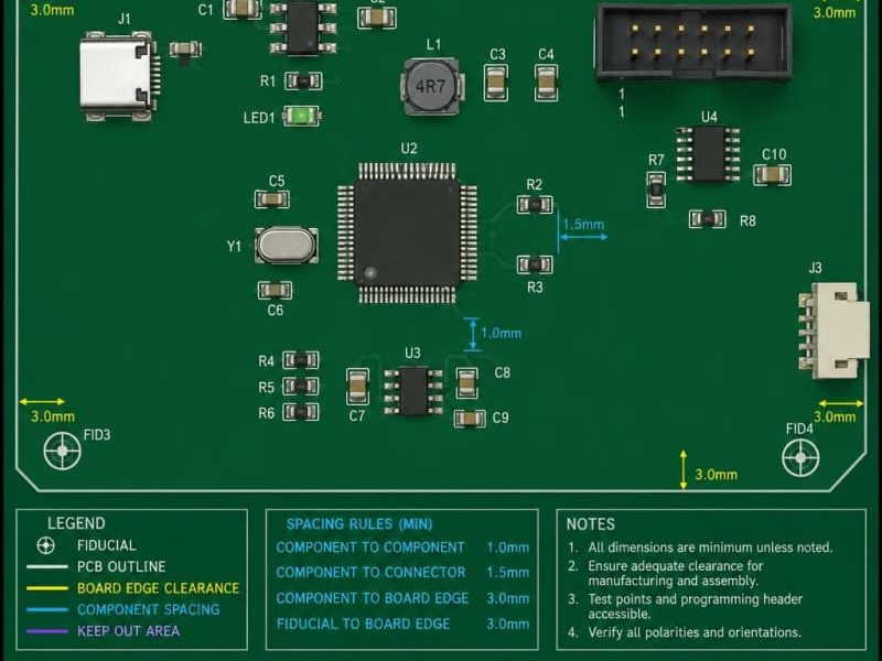
PCB design for assembly is the discipline of creating a board that can be built reliably, inspected efficiently, and scaled without avoidable rework. Strong design for assembly decisions begin long before a PCB reaches the assembly line: component choices, footprints, spacing, panelization, soldering method, and documentation all shape whether production is smooth or frustrating. This guide explains practical pcb design for assembly guidelines you can use to reduce ambiguity, support the pcb manufacturing process, and create boards that are easier to quote, source, assemble, test, and repeat.
What does PCB design for assembly mean?
PCB design for assembly means designing the printed circuit board with the actual assembly process in mind, not only the electrical schematic or board outline. A design may function electrically but still be difficult to build if parts are too close together, footprints are unclear, polarities are ambiguous, or documentation leaves the assembler guessing. DFA design for assembly helps bridge the gap between engineering intent and a reliable physical product.
In practical terms, pcb design for assembly focuses on whether components can be placed, soldered, inspected, cleaned if required, and tested using the chosen manufacturing methods. It asks questions such as: Can pick-and-place equipment access the parts? Are fiducials available for alignment? Is there enough clearance around tall or heat-sensitive components? Are all parts available in assembly-friendly packaging? These concerns are not cosmetic; they affect yield, cost, lead time, and the likelihood of late-stage changes.
Excellent PCB Design Companies treats assembly as a design input, not a final handoff. The earlier you involve your assembler or contract manufacturer, the easier it is to catch risks while they are still inexpensive to fix. Once boards are fabricated and components are purchased, even small layout issues can become expensive delays.
Assembly-aware decisions start at the schematic
Many assembly problems are created before layout begins. The schematic stage is where the bill of materials takes shape, component packages are selected, and electrical requirements become physical constraints. If design for assembly is ignored here, the layout team may inherit parts that are hard to source, difficult to solder, or unnecessarily complex to inspect.
Choose components with availability, package style, and assembly method in mind. Standard surface-mount packages are usually easier to automate than unusual or highly specialized packages, assuming they meet the electrical and mechanical needs of the design. If a component requires hand soldering, selective soldering, special handling, or unusual thermal control, document that early and confirm the assembler can support it.
Footprint selection also begins at the schematic-library level. A footprint should match the exact manufacturer package or an approved land pattern, not a visually similar part. Small mismatches in pad size, pitch, courtyard, or pin numbering can lead to soldering defects, reversed parts, or inspection confusion. Library discipline is one of the most valuable pcb design best practices because it prevents errors from being copied into every future revision.
Before layout, review the BOM for risk. Look for lifecycle concerns, single-source parts, unclear manufacturer part numbers, incompatible package types, and parts that are not supplied in production-friendly packaging. A clean BOM helps the assembler verify parts quickly and reduces the chance of substitutions being made under pressure.
Layout practices that make boards easier to build
A layout built for assembly is organized, readable, and manufacturable. It still satisfies electrical performance requirements, but it also gives machines, operators, and inspectors enough room and information to do their jobs. The goal is not to make every board spacious; it is to use space intentionally.
Maintain practical component spacing
Component spacing affects placement accuracy, solder joint formation, inspection access, and rework. Parts placed too close together can create solder bridging, shadowing during soldering, or blocked access for probes and tools. Crowded placement can be especially challenging around connectors, shields, large electrolytic capacitors, heat sinks, and fine-pitch packages.
Follow your assembler’s spacing rules whenever available. If no specific rules are provided, keep adequate courtyards around each component and avoid placing tall parts where they obstruct smaller neighboring parts. Orient similar components consistently when possible, which supports automated optical inspection and makes manual review easier.
Use footprints and land patterns carefully
Footprints are one of the highest-risk areas in pcb design for assembly. A correct schematic symbol cannot compensate for an incorrect land pattern. Pads that are too large may encourage tombstoning or excess solder; pads that are too small may weaken joints or reduce inspection visibility. Incorrect pin numbering can create a board that is assembled perfectly but functions incorrectly.
Use controlled libraries, review new footprints against manufacturer drawings, and include polarity, pin-one, and orientation indicators on the silkscreen or assembly drawing. For connectors, switches, and mechanical parts, confirm the footprint with the 3D model or mechanical drawing. This prevents conflicts with enclosures, mating cables, and user-accessible features.
Plan component orientation for assembly flow
Consistent orientation improves assembly efficiency and inspection clarity. Where circuit performance allows, align polarized components in a common direction and place IC pin-one markers consistently. This reduces the cognitive load on reviewers and helps inspection systems compare expected and actual placement.
Orientation also matters during soldering. Some components may be more sensitive to thermal imbalance, tombstoning, or solder wicking depending on pad design and placement. When using small passive components, balanced pad geometry and symmetrical copper connections can help reduce uneven heating.
Provide fiducials and tooling support
Fiducials help automated equipment align the board during solder paste printing and component placement. Global fiducials support the full board, while local fiducials can help with fine-pitch devices or dense areas. They should be unobstructed, clearly defined, and placed according to the assembler’s rules.
Tooling holes, breakaway rails, and panel features may also be required depending on the board size, shape, and production equipment. Do not treat panelization as an afterthought. A board that is electrically correct but difficult to fixture may require extra handling or custom tooling.
How does DFA affect the PCB manufacturing process?
DFA affects the pcb manufacturing process by reducing uncertainty at each step: fabrication, solder paste application, component placement, soldering, inspection, test, and rework. When the design provides clear spacing, reliable footprints, usable fiducials, complete documentation, and realistic assembly constraints, the manufacturer has fewer assumptions to make. That can improve build repeatability and make problems easier to diagnose if they occur.
The pcb manufacturing process usually involves more than simply fabricating copper layers and attaching parts. Bare boards must be manufactured to the right stackup, finish, hole sizes, solder mask clearances, and controlled features. During assembly, solder paste must be applied accurately, components must be placed correctly, and solder joints must form under the selected thermal profile. Each stage depends on decisions made during design.
For example, a dense board with fine-pitch ICs may require tighter control of solder paste stencil design and inspection access. A board with heavy copper areas connected to small passive pads may heat unevenly during reflow. A design that mixes many through-hole and surface-mount parts may require additional process steps. None of these choices is automatically wrong, but they should be intentional and documented.
Good pcb design for assembly guidelines also help control revision churn. If your assembler identifies a spacing violation, missing polarity mark, or unsuitable package after release, the project may need design changes, new fabrication files, updated purchasing, and schedule adjustments. A DFA review before release is far less disruptive.
Documentation that prevents assembly mistakes
Clear documentation is part of the design, not an administrative extra. The assembler should not have to infer critical details from incomplete files or conflicting notes. A complete release package helps ensure that the board built matches the board intended.
A typical assembly documentation package may include fabrication files, assembly drawings, BOM, centroid or pick-and-place file, approved substitutions if any, special handling notes, test requirements, and revision information. If a component orientation could be misunderstood, show it clearly. If a part must be mounted at a specific height, soldered by hand, left unpopulated, or installed after cleaning, state that directly.
Essential release checks
Use this pcb design for assembly checklist before sending a design for quote or production:
- BOM clarity: Include manufacturer part numbers, approved alternates where applicable, reference designators, quantities, descriptions, and package information.
- Footprint verification: Confirm every new or modified footprint against the component datasheet or manufacturer drawing.
- Polarity and pin-one marking: Check diodes, LEDs, electrolytic capacitors, ICs, connectors, batteries, and any asymmetric components.
- Centroid file accuracy: Verify coordinates, rotation, side of board, and reference designators.
- Fiducials and tooling: Confirm global fiducials, local fiducials if needed, panel rails, and tooling holes with the assembler.
- Component spacing: Review courtyards, height conflicts, connector access, rework access, and inspection visibility.
- Soldering method: Confirm whether parts are compatible with reflow, wave, selective, or manual soldering as required.
- Test access: Ensure required nets have accessible test points or another defined test method.
- Revision control: Make sure all files, drawings, and BOMs carry matching revision identifiers.
- Special instructions: Document no-clean requirements, conformal coating keepouts, masking, hand operations, or do-not-populate parts.
This checklist is not a replacement for assembler-specific rules. It is a starting point that helps catch common issues before the design leaves engineering.
Component selection shapes assembly quality
Component selection influences more than electrical performance. It determines placement method, solderability, inspection options, sourcing flexibility, and repair difficulty. A part that looks ideal in a schematic may create unnecessary assembly burden if it comes in a difficult package or lacks supply stability.
Prefer packages that fit the production volume and available process. For prototypes, a slightly larger package may make debugging and rework easier. For mature products, smaller packages may be justified if the assembler can place and inspect them consistently. The right choice depends on the product, not on package size alone.
Packaging format matters as well. Tape-and-reel, cut tape, trays, tubes, or bulk packaging can affect handling and machine setup. If production will be automated, confirm how parts should be supplied. Supplying components in a format that does not suit the equipment may add labor or risk.
Also consider whether components are moisture-sensitive, ESD-sensitive, temperature-sensitive, or mechanically fragile. These parts may require special storage, baking, handling, or process controls. If such requirements are real for your chosen parts, communicate them in the BOM and assembly notes instead of assuming they will be discovered later.
Design rules for soldering, inspection, and rework
Assembly guidelines should account for how solder joints are formed and verified. Soldering is a physical process affected by pad geometry, copper balance, thermal mass, component size, board finish, and process profile. Inspection and rework then depend on whether the resulting joints are visible and accessible.
Support reliable solder paste printing
For surface-mount assembly, solder paste printing is a critical step. Dense components, very small passives, large exposed pads, and fine-pitch leads may need careful stencil aperture design. While the assembler often defines final stencil details, the PCB layout should make that work possible by using appropriate pads, solder mask clearances, and component spacing.
Avoid unnecessary solder mask slivers between tightly spaced pads if they cannot be manufactured reliably. Confirm solder mask expansion rules with the fabricator. For exposed-pad components, provide via-in-pad or thermal via strategies only when they are compatible with the assembly process and properly specified.
Make inspection possible
Automated optical inspection and human inspection both depend on visibility. Silkscreen should not cover pads, hide polarity marks, or crowd reference designators into unreadable spaces. Reference designators do not have to fit perfectly beside every tiny part on the board, but the assembly drawing should make every part identifiable.
For packages with hidden solder joints, such as some bottom-terminated components, inspection may require X-ray or process controls. If the design includes these packages, discuss inspection expectations with the assembler. Hidden joints are common in modern PCB design, but they should not be used casually when simpler packages can meet the requirement.
Preserve rework access where it matters
Not every product needs easy field rework, but prototypes and early builds often do. Leave access around parts likely to be changed during validation, such as configuration resistors, connectors, sensors, power components, and programming headers. Crowding these areas can slow debugging and increase the chance of board damage during modification.
For production boards, rework access still matters around expensive, sensitive, or failure-prone components. If a part cannot realistically be reworked once installed, the design and process should be reviewed more carefully before release.
Testability is part of assembly readiness
A board that cannot be tested efficiently can create bottlenecks after assembly. Testability should be considered during placement and routing, not after the layout is complete. Even simple test points can make a major difference during bring-up, programming, and production screening.
Place test points on important power rails, ground, programming interfaces, communication lines, reset lines, and signals needed for functional verification. Keep them accessible to probes or fixtures and avoid placing them under tall components, shields, or areas blocked by the enclosure. If bed-of-nails testing is planned, confirm pad sizes, spacing, and side-of-board requirements with the test fixture provider.
Test documentation should explain what needs to be verified, not merely provide raw access. Define programming steps, pass/fail expectations, connector use, and any calibration or configuration requirements. If a board has multiple assembly variants, make sure the test process can distinguish them.
When should you involve your assembler?
You should involve your assembler before the design is released, ideally while component selection and placement can still change. Early feedback can identify package risks, spacing concerns, panelization needs, soldering constraints, inspection limitations, and documentation gaps. The later this review happens, the more expensive and disruptive the changes become.
A productive DFA review is not just a file upload at the end of layout. Share the intended production volume, prototype goals, soldering method, special components, mechanical constraints, and any known risks. If the board has unusual features such as heavy copper, rigid-flex construction, press-fit connectors, conformal coating, or high component density, discuss them directly.
Use the assembler’s feedback to refine your internal pcb design best practices. Over time, repeated issues should become library rules, checklist items, or design constraints. This turns lessons learned into a stronger design system instead of relying on individual memory.
Common DFA mistakes to avoid
Many assembly problems come from small oversights rather than complex engineering failures. A careful review can catch these issues before they reach production.
- Using unverified footprints: Always confirm land patterns, pin numbering, and mechanical dimensions before release.
- Leaving polarity ambiguous: Make orientation obvious on the board or assembly drawing, especially for polarized and asymmetric parts.
- Ignoring component height: Check enclosure clearance, neighboring component access, and soldering equipment limitations.
- Crowding connectors: Leave room for mating cables, latch movement, fingers, tools, and strain relief.
- Skipping test points: Provide access for bring-up, programming, diagnostics, and production test.
- Mixing processes unnecessarily: Combining many assembly methods can add handling unless the product truly requires it.
- Poor revision control: Mismatched BOMs, Gerbers, and placement files can cause the wrong board to be built correctly.
- Treating DFM and DFA separately: Fabrication and assembly constraints interact, so review them together whenever possible.
Avoiding these mistakes does not require overdesigning the board. It requires making assembly needs visible during normal design decisions.
A practical PCB design for assembly workflow
The most reliable approach is to build DFA into each design phase instead of saving it for a final checklist. Begin with assembly-friendly component choices, continue with controlled footprints and placement rules, and finish with a complete documentation review. This creates a repeatable workflow that supports both prototypes and production builds.
A simple workflow looks like this:
- Define assembly assumptions early. Decide expected build volume, soldering method, inspection needs, and prototype versus production priorities.
- Review the BOM before layout. Check part availability, package suitability, approved alternates, and special handling requirements.
- Verify footprints before placement. Compare land patterns with manufacturer drawings and confirm orientation markings.
- Place for process and access. Account for spacing, height, fiducials, tooling, connectors, thermal issues, and rework needs.
- Route without blocking testability. Preserve access to required nets and avoid creating avoidable inspection or soldering challenges.
- Run internal design checks. Use electrical, mechanical, fabrication, and assembly reviews rather than relying on one final pass.
- Get assembler feedback. Send preliminary files when changes are still practical.
- Release a synchronized package. Ensure the BOM, placement file, fabrication data, drawings, and notes all match the same revision.
This workflow keeps pcb design for assembly practical. It does not slow the project down; it helps prevent late surprises that are harder to fix.
Key takeaways for better assembly outcomes
Design for assembly is about reducing friction between the digital design and the physical build. The best results come from clear component choices, verified footprints, practical spacing, readable documentation, and early collaboration with the manufacturer. A board that is easy to assemble is also easier to inspect, test, troubleshoot, and improve.
Use a pcb design for assembly checklist on every release, even for familiar designs. Small layout changes can introduce new assembly risks, and repeated products can still suffer from documentation drift or component substitutions. Treat DFA as part of engineering quality, not just manufacturing preference.
When in doubt, feel free to contact Greenpcba Technology directly, learn what need to build the board consistently. Our process knowledge can turn a functional design into a production-ready design, and that is the real purpose of strong pcb design for assembly guidelines.
Recent Comments