
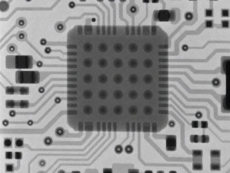
A PCB X-ray machine helps manufacturers, repair teams, and quality engineers inspect hidden solder joints, internal layers, and electronic components without cutting into the board. It is one of the most useful forms of non-destructive testing for modern electronics, especially when defects cannot be seen with optical inspection alone. As a professional one-stop electronics manufacturer, Greesnpcba technology will explains how PCB X-ray inspection works, where it fits among PCB testing equipment, and what to consider before choosing a system.
What does a PCB X-ray machine actually do?
A PCB X-ray machine sends controlled X-rays through a circuit board and captures an image based on how different materials absorb the radiation. Dense materials, such as solder and metal leads, appear differently from lighter materials, allowing operators to see beneath components and inside solder connections. In practical terms, x ray machine PCB inspection helps reveal hidden issues such as voids, bridges, misalignment, insufficient solder, and internal connection problems.
This matters because many assemblies now use packages that hide their joints underneath the component body. Ball grid arrays, QFNs, LGAs, and dense multilayer boards may look acceptable from the outside while still containing internal defects. A circuit board X ray machine gives inspection teams a view they cannot get from microscopes or cameras alone.
Why X-ray inspection has become important in electronics
Electronics have become smaller, denser, and more complex. As components shrink and more connections move underneath packages, traditional visual inspection reaches its limits. X-ray inspection systems help bridge that gap by showing the internal condition of the assembly before a defect becomes a field failure.
A pcb x ray inspection machine is especially useful in environments where reliability matters, such as industrial controls, automotive electronics, medical devices, aerospace assemblies, and high-value consumer products. Even in lower-volume production or repair settings, X-ray inspection can reduce guesswork and support more confident decision-making.
The value is not just in finding obvious failures. A good inspection process can also identify process trends, such as repeated voiding in a solder joint or consistent component placement drift. That makes X-ray inspection useful for both quality control and process improvement.
Common defects found with PCB X-ray inspection
A pcb x ray machine can support many inspection tasks, depending on the board design, component package, and system capability. Typical findings include:
- Solder voids: Empty spaces inside solder joints that may affect thermal or electrical performance.
- Bridging: Unwanted solder connections between adjacent pads, balls, or leads.
- Open joints: Missing or incomplete solder connections that interrupt the circuit.
- Head-in-pillow defects: Poor contact between a BGA ball and solder paste, often difficult to detect visually.
- Misaligned components: Packages or leads that shifted during placement or reflow.
- Insufficient or excessive solder: Joint conditions that may signal process control issues.
- Internal layer or via problems: Certain structural issues that may be visible depending on board construction and system resolution.
These findings make X-ray inspection for electronic components valuable during production, troubleshooting, and root-cause analysis. It does not replace every electrical or functional test, but it adds a powerful internal view that other methods cannot provide.
How does automatic X-ray inspection differ from manual inspection?
Automatic X-ray inspection uses software, motion control, and programmed inspection routines to evaluate boards more consistently than a fully manual process. Instead of relying only on an operator to move the sample and interpret every image, automatic x ray inspection can compare features against defined criteria, flag suspicious areas, and generate repeatable results. For high-volume production, automated x ray inspection can save time and reduce variation between inspectors.
Manual inspection still has a place. Skilled operators are often needed for unusual boards, failure analysis, prototype review, and final interpretation of complex images. However, automatic x ray inspection PCB workflows are useful when the same product must be checked repeatedly and consistently.
A practical approach often combines both methods. Automated routines handle repetitive checks, while engineers review exceptions, tune thresholds, and investigate failures. This balance can improve throughput without removing human judgment from the process.
Where PCB X-ray fits in a testing workflow
A PCB X-ray machine is most effective when it is part of a broader quality strategy. It should complement, not replace, other inspection and testing tools. Each method sees a different part of the problem.
A typical workflow may include:
- Visual inspection to catch obvious placement errors, missing parts, polarity issues, or surface contamination.
- Automated optical inspection for fast checks of visible component features and solder fillets.
- X-ray inspection for hidden joints, internal solder conditions, and concealed package defects.
- Electrical testing to confirm continuity, shorts, programming, and functional behavior.
- PCB failure analysis when a board fails and the team needs to understand why.
In this sequence, X-ray inspection acts as a bridge between appearance and performance. It helps explain why a circuit may fail even when the surface looks acceptable, and it can prevent unnecessary destructive analysis when the issue is visible internally.
Key features to consider in a PCB X-ray inspection machine
Not every system is designed for the same workload. Before selecting a pcb x ray inspection machine, it helps to match the equipment to the boards, components, and inspection goals.
Important considerations include:
- Resolution and magnification: Needed for fine-pitch components, small solder balls, and dense assemblies.
- 2D or 3D capability: 2D systems are useful for many tasks, while 3D or CT-style inspection can help separate overlapping features.
- Board size capacity: The inspection area must fit the assemblies you produce or repair.
- Software tools: Measurement, void calculation, defect recognition, and reporting features can improve consistency.
- Automation level: Manual, semi-automatic, and fully automatic x ray inspection systems serve different production needs.
- Ease of use: Clear controls, stable imaging, and efficient sample handling matter in daily operation.
- Safety design: Shielding, interlocks, and compliance features are essential for responsible use.
The best choice is not always the most complex system. A repair lab may need flexible manual control, while a production line may prioritize repeatability, speed, and automatic defect detection.
What should teams know before using X-ray for PCB failure analysis?
Teams should know that X-ray inspection is powerful, but image interpretation requires context. A dark or light area on an image is not automatically a defect; it must be evaluated against the component type, solder joint design, process history, and acceptance criteria. For PCB failure analysis, X-ray results are most useful when combined with electrical symptoms, production records, and physical inspection.
It is also important to define what the inspection is meant to answer. Are you checking for solder voids, confirming BGA alignment, looking for a short, or investigating an intermittent failure? Clear goals help operators choose the right angle, magnification, exposure settings, and inspection method.
Documentation matters as well. Captured images, measurements, and notes create a record that engineers can compare across boards or use when discussing corrective actions. Over time, this information can reveal whether a defect is isolated or part of a larger process pattern.
Practical tips for better inspection results
Good equipment helps, but process discipline makes the inspection more valuable. Teams can improve results by standardizing how they use their circuit board X ray machine and by training operators to understand both the image and the assembly.
Helpful practices include:
- Create inspection recipes for repeat products so settings are consistent.
- Use known-good boards as references when evaluating new defects.
- Capture images at multiple angles when overlapping features make interpretation difficult.
- Avoid judging acceptability from appearance alone; connect findings to design and reliability requirements.
- Review recurring defects with process engineers, not just inspection staff.
- Keep reports clear enough for production, engineering, and customers to understand.
These habits turn inspection from a pass-fail checkpoint into a source of practical manufacturing insight.
The takeaway
A PCB X-ray machine gives electronics teams a non-destructive way to see hidden features, verify solder quality, and support faster troubleshooting. Whether used for production control, repair work, or PCB failure analysis, it fills an important gap between visual checks and electrical tests.
For organizations evaluating PCB testing equipment, the right choice depends on board complexity, inspection volume, component types, and reporting needs. When used with clear goals and trained interpretation, x-ray inspection systems can improve confidence in both the product and the manufacturing process.
Recent Comments