

From Rapid Prototyping to Mass Production
Are you struggling with poor soldering quality, delayed lead times, or manufacturers who won’t accept low-volume orders? At Greenspcba, we bridge the gap between high-end precision and flexible manufacturing. We don’t just place components; we ensure your hardware’s heartbeat is stable.
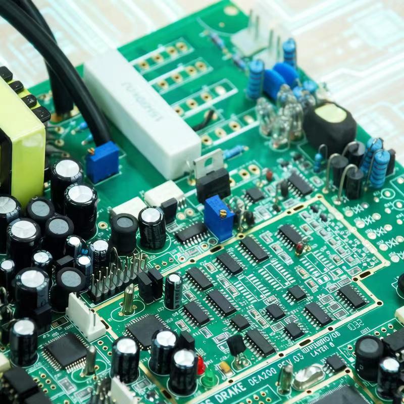
Why Choose Our SMT Assembly for Your Mission-Critical Electronics?
In the PCBA industry, “Standard” is the bare minimum. We go beyond by offering specialized SMT solutions for industries where failure is not an option: Medical, Automotive, and Industrial IoT.
Our Technical Edge
01005 & Fine-Pitch Expertise: Precision placement for the smallest passive components and ultra-fine pitch BGAs ($0.3mm$ pitch).
We don’t guess. Every BGA solder joint is verified via X-Ray to eliminate voids and hidden bridges.
IPC Class 2 & 3 Compliance
Whether it’s consumer-grade or mission-critical industrial grade, we adhere strictly to IPC-A-610 standards.

Capabilities & Equipment: Built for Precision
We’ve invested in high-speed, high-accuracy lines to ensure your project moves from Gerber to functional PCBA in record time.

| Feature | Specification / Capability |
| Component Size | Min: 01005 (0402 metric); Max: 74mm sq. |
| Placement Accuracy | $\pm 0.025mm$ (High-speed Pick & Place) |
| Max PCB Dimensions | 500mm x 450mm |
| PCB Layers | 1 to 32 layers |
| Soldering Environment | Nitrogen ($N_2$) Reflow available for oxidation-sensitive parts |
| Testing Services | AOI, X-Ray, ICT, and Full Functional Testing (FCT) |
The Professional SMT Process: How We Guarantee Quality
Many small factories skip steps to save costs. We prioritize Process Integrity to protect your cash flow from costly rework.
Before we touch the board, our engineers review your files to catch design errors that cause soldering defects.
Solder Paste Printing
Using high-precision stencils and SPI (Solder Paste Inspection) to ensure the foundation of every joint is perfect
Automated Pick & Place
High-speed mounting with vision-correction systems for flawless alignment.
Optimized Reflow Profile
We customize temperature curves for every board, preventing thermal shock to sensitive ICs.
Multi-Stage Inspection
A combination of 3D AOI and manual QC ensures 100% yield before shipping.
Frequently Asked Questions (FAQ)
To provide an accurate quote within 24 hours, we require:
- Gerber Files (RS-274X format) including RS-274X, Silkscreen, and Solder Mask layers.
- BOM (Bill of Materials) with manufacturer part numbers (MPN) and descriptions.
- Pick-and-Place file (XY Data).
- Quantity and any special testing requirements (e.g., FCT or X-Ray).
Absolutely. We specialize in supporting startups and R&D teams. We have no Minimum Order Quantity (MOQ). Whether you need 1 board for functional testing or 500 for a pilot launch, we treat both with the same level of IPC-compliant precision.
We use a 100% Automated Optical Inspection (AOI) coverage for every board. For BGA, QFN, and other leadless components, we perform X-Ray inspection to verify solder ball integrity, checking for voids, bridging, or cold solder joints that the naked eye cannot see.
We offer three flexible options:
- Turnkey: We source all components from authorized distributors (Digi-Key, Mouser, Arrow).
- Consigned: You ship all components to us.
- Partial Turnkey: You provide the “key” ICs, and we source the common resistors and capacitors.
- Prototype: 3–5 working days (after all components are in stock).
- Mass Production: Typically 2 weeks, depending on complexity and volume. We also offer Express 24-hour service for urgent R&D deadlines.
We take IP security seriously. We are happy to sign a Non-Disclosure Agreement (NDA) before you share any design files. Internally, access to client data is strictly controlled and used only for manufacturing purposes.